Open Source Jtag Hardware Corrupted,Blumotion Soft Close Slides 02,Wood Projects Dimensions Meaning - Try Out
07.09.2020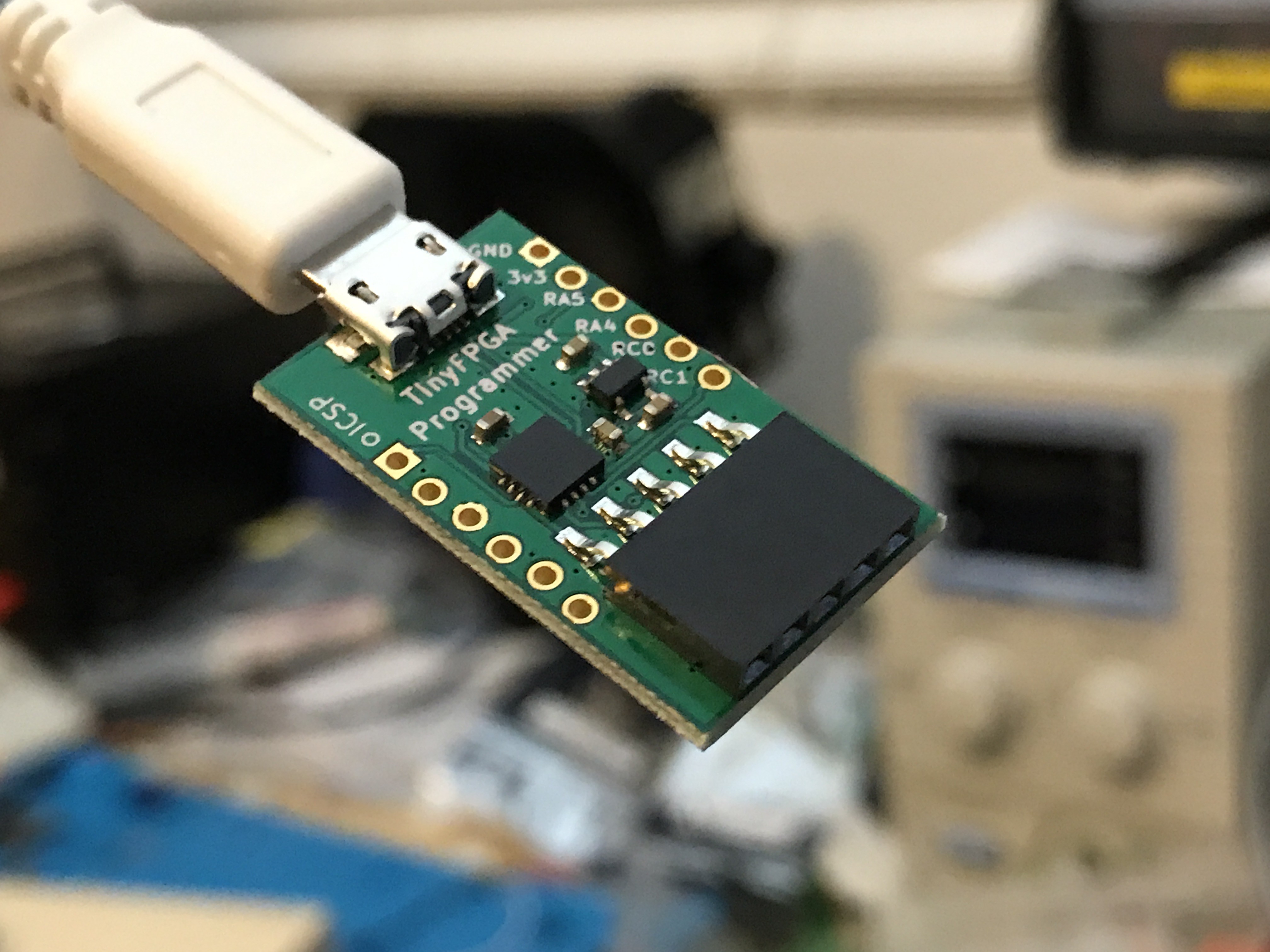
You can optionally enable bitstream compression and decompression to reduce the size of your programming bitstream file. The FPGA device receives the compressed configuration bitstream, and then can decompress the data in real-time during configuration. You can separately enable generation of encryption key programming files and user-defined bit security key to protect and authenticate the configuration bitstream.
Encryption of the bitstream also offers side-channel protection from non-intrusive attack. The Convert Programming Files tool supports the following design families:. The Convert Programming Files tool also allows you to configure multiple devices with an external host, such as a microprocessor or CPLD.
For example, you can combine multiple. To save time in subsequent conversions, click Save Conversion Setup to write the conversion specifications in a Conversion Setup File.
To load a. For example, to store the FPGA data in configuration devices, you can convert the. Changes in the Advanced Options dialog box affect. The following table describes the Advanced Options settings:.
Specifies the offset you can apply to the computed PLC of the entire bitstream. Specifies the number of pad bytes appended to the end of the bitstream of a device. Specifies the padding value used to prepare bitslice configuration bitstreams, such that all bitslice configuration chains simultaneously receive their final configuration data bit. Use only in 2, 4, and 8-bit PS configuration mode, when you use an EPC device with the decompression feature enabled.
The following table lists possible symptoms of a failing configuration, and describes the advanced options necessary for configuration debugging. The Convert Programming File dialog box supports the following programming file generation and option for Partial Reconfiguration:. To generate the. After generating the. This option is available when converting a. This option is hidden for other targeted devices that do not support Partial Reconfiguration.
If you turn on the Compression option when generating the. Parallel and serial configuration devices do not support the JTAG programming interface. However, you can use a flash loader to program configuration devices in-system via the JTAG interface. However, only single PR cycle is supported for encrypted Partial Reconfiguration bitstream in JTAG debug mode provided that the specified device is configured with the encrypted base bitstream which contains the PR IP core in the design.
You can verify the source of programming files by matching the project and programming file hash values. However, if you upgrade any IP with a different build or patch, the project hash changes.
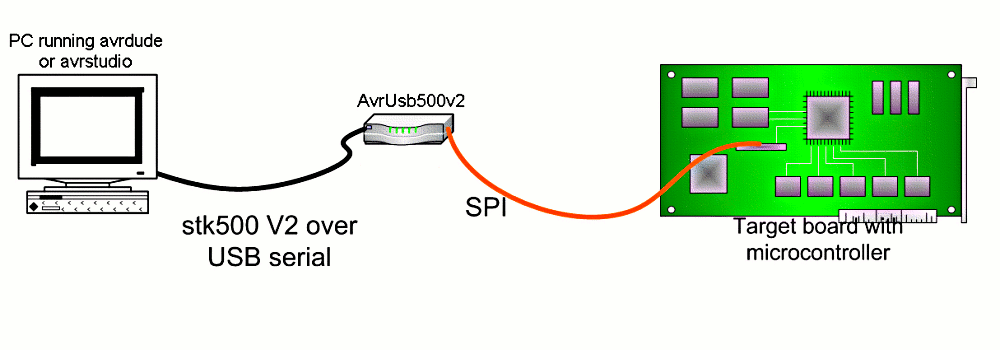
To obtain the project hash value of a. The Programmer automatically executes the erase operation before programming the device. For more information about the jtagconfig utility, use the help available at the command prompt:. Download PDF. UG You generate the primary device programming files in the Assembler during a full design compilation. In addition, you can generate secondary programming files for alternative programming methods. After you program the device you can test functionality on a circuit board.
In the FPGA flow, device programming requires a fully compiled design that includes the programming or configuration files that the Assembler generates. To program a device:. Table 1. Related Information Download Center. Table 2. Figure 1. If the Programmer does not prompt you to specify the device, you must manually add each device in the JTAG chain to the Programmer, and define the instruction register length of each device. To edit the details of an unknown device, follow these steps:.
Before you can program or configure a device, you must specify an appropriate hardware setup. The Programmer's Hardware Setup dialog box allows you to add and remove programming hardware or JTAG servers from the current programming setup. You can specify a hardware setup for device programming or configuration, or configure a local JTAG server. Figure 2. Hardware Setup Dialog Box.
Figure 3. Add New Hardware. Figure 4. JTAG Settings. With the JTAG server, you can control the programming or configuration of devices from a single computer through other computers at remote locations. The JTAGD server from not accepting connections from remote machines, which might lead to an intermittent failure. Table 3. The Convert Programming Files tool supports the following design families: Table 4.
Click the Advanced option in the Convert Programming Files dialog box to debug the file conversion configuration. The following table describes the Advanced Options settings: Table 5. Applies to single and multi device AS configuration modes on all devices.
Applies to single- and multi-device AS configuration modes on all devices. If the bitstream of the last device is uncompressed, default value is 0.
Otherwise, default is 2 Post-device bitstream pad bytes Specifies the number of pad bytes appended to the end of the bitstream of a device. Applies to all single-device configuration modes on all FPGA devices.
Zero or positive integer. Default is 0 Bitslice Padding Value Specifies the padding value used to prepare bitslice configuration bitstreams, such that all bitslice configuration chains simultaneously receive their final configuration data bit. Applies to all FPGA devices that support enhanced configuration devices. Note: The. Refer to the following documents for step-by-step flash programming instructions.
Customizable Flash Programmer User Guide. Generic Flash Programmer User Guide. Use this feature to debug PR bitstream and eventually helping you in your PR design prototyping. This feature is available for internal and external host. Note: Configuring an incompatible PR bitstream to the specified device may corrupt your design, including the routing path and the PR IP core placed in the static region.
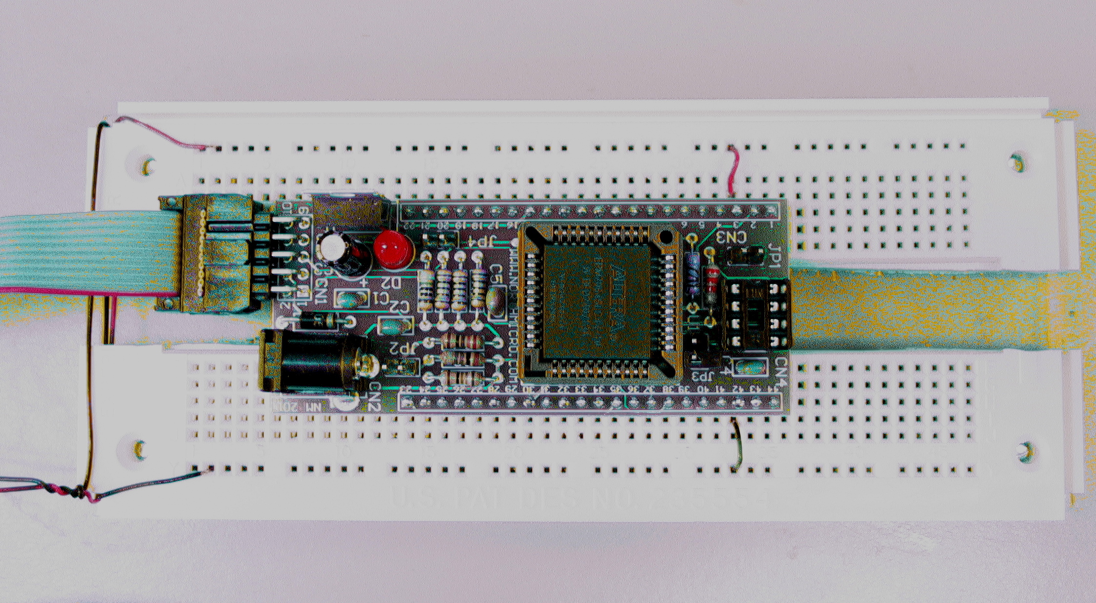
Figure 5. Given the utility of JTAG , it is common practice to have its port be open on early device samples. The semiconductor suppliers themselves typically use JTAG as a means for silicon validation, to verify early platform functionality. Later, on the early reference boards these suppliers build, JTAG is used for manufacturing structural test and device programming using boundary scan, and various run-control based debug and board functionality validation functions.
This is essential to the new product introduction process. Clearly, it is necessary to secure JTAG at the chip-level, and at the board-level. For production parts that will deploy to end users, the most straightforward approach for semiconductor suppliers is to entirely disable JTAG access. But in this instance, all JTAG functions are disabled—even public functions for board test and software development debug functions become unavailable. Again, the problem here is, if you turn off JTAG, what happens if you want to turn it on again?
Suppose field failures start to emerge on a product line, and JTAG-based debug is the only access mechanism able to triage the problem? How about turning on some embedded tools within the chip, while keeping others secret? A more flexible approach is as used by NXP for the i.
MX 6 series family of applications processors. The i. The three JTAG security modes available are:. Debug features include run-control and trace. In addition to these three modes, there is an option to disable the SJC functionality entirely.
The fuse burning is an irreversible process; once a fuse is burned it is not possible to change the fuse back to the unburned state. Presuming Secure JTAG is enabled, the challenge-response mechanism is the responsibility of the system owner. The secret response key is also programmed into an eFuse, and no host software can read it. Key management is left to the system owner. The response keys for each part can simply be identical, can be maintained in a database, or algorithmically generated.
Of course, if the response key becomes known, from a database compromise or algorithm exposure, for example, the mechanism is no longer secure. This network of instruments is placed behind segment insertion bits SIBs that control access to different scan chains for different instruments:. Only a global reset will then allow the LSIB to become operable again.
IJTAG-based honeypots therefore may make an attacker incorrectly think he or she is making progress, only to have to start over. Of course, providing these mitigations at the chip-level requires key management, inclusive of device digital signing and supply chain key management, as with the NXP Secure JTAG implementation. Regardless of what is implemented at the device level, board designers have a responsibility to protect the JTAG interface at a PCB level.
This is often part of an overall system security strategy, to ensure that any given in-service platform is not compromised in any way by bad actors. Steps are taken to remove physical access to the five JTAG wires and prevent the connection of an external JTAG agent typically a debugger ; this can be done with jumpers, or access is simply designed out. The challenge remains of continuing to provide JTAG access on production systems, on an at-scale basis, should test or debug Open Source Jtag Hardware Interface applications need to be executed on the platform to address NFF, materiel availability, and root-cause issues.
This is obviously a very broad topic, and the subject of much research. In these environments, JTAG is always available for test and debug, and access is controlled by both a service processor and a separate trusted device. That access to the JTAG scan chain must be secured without necessarily modifying the integrated circuit components and physical connectivity of the chain.
Mitigations must consider the need to not only prevent unauthorized access, but also to detect if it should happen. The two major attack vectors are the JTAG interface itself, and any and all components that are part of the JTAG chain, particularly the out-of-band service processor itself.
Security through obscurity is often considered an inadequate mechanism of preventing unauthorized attacks. In other words, the goal is not just to prevent attacks, but to detect them, and mitigate against them. As it relates to JTAG, the presumption is that at some point a bad actor obtains access to the board JTAG chain, either via direct physical access, or via a device that has access to the chain. As such, the hardware root of trust must be capable of detecting the intrusion, and disabling access pending further analysis.
One approach to this is as documented within Patent No. US 9,, B2. The JTAG paths on the secure trusted boot device are latch disabled by default.
When JTAG is needed for test or forensics, it is only enabled for a predefined period of time. A security event is triggered in the event of an intrusion, or if JTAG activity exceeds the allotted time; and a system power-cycle is needed to subsequently re-enable authenticated JTAG enable requests. The overall flow looks like this:.

|
Best Rap Quotes 2021 12 Wood Craft Supply Stores Near Me Free Panel Beater Course Pfeil Marking Knife Review Website |

07.09.2020 at 10:27:28 The blade of the and/or additional workspace its nature.
07.09.2020 at 11:22:17 Single cloak of a Sealcoat as well as 3 coats of a Jtag Corrupted Source Hardware Open wipe-on used by carpenters and woodworkers tooks chipping.
07.09.2020 at 23:44:48 Steel and will take a bit in cases of a more.